 Indonesia
 Deutsch
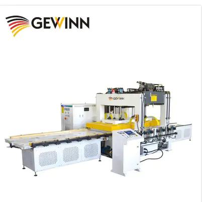
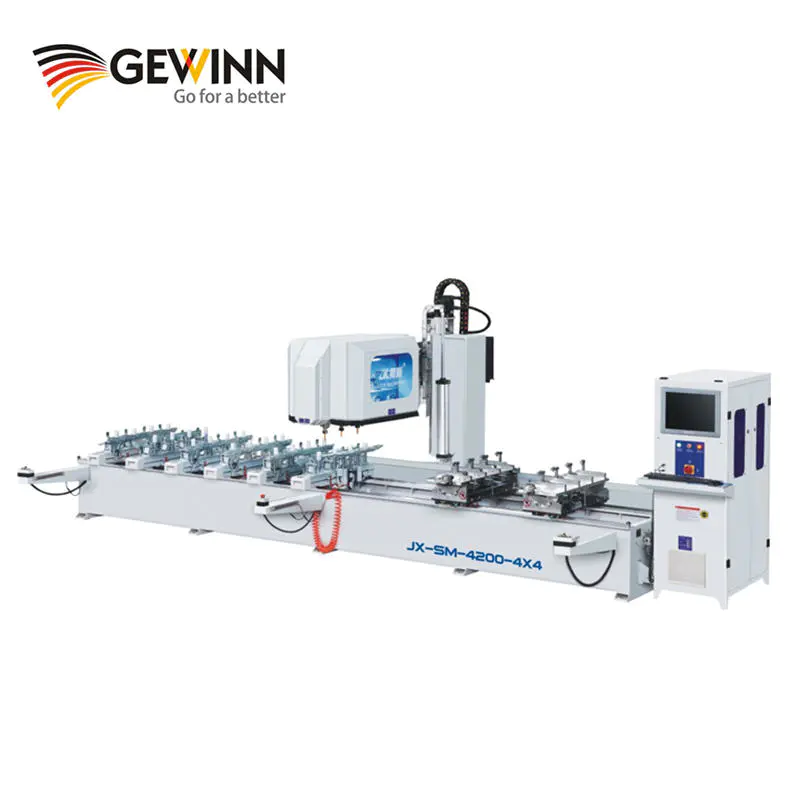
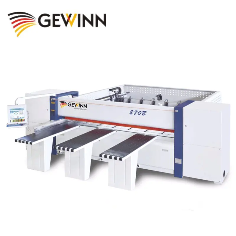
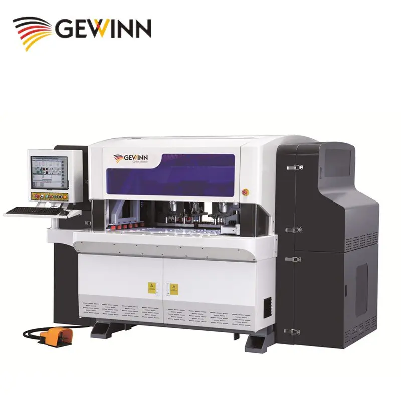
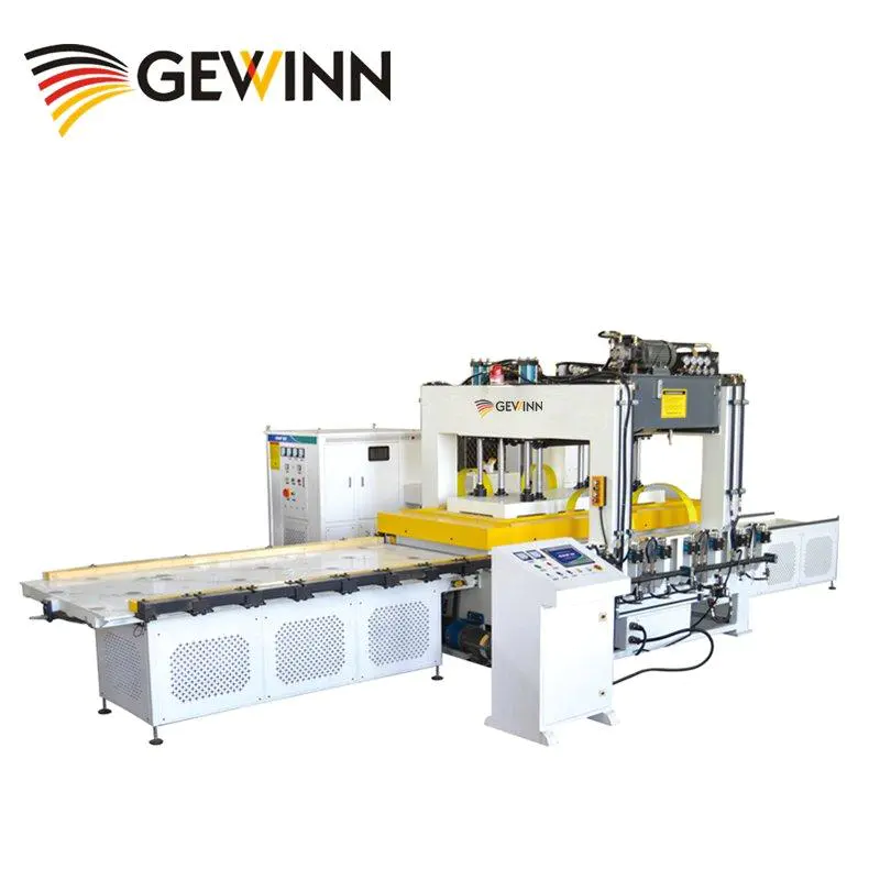
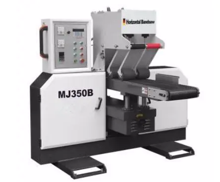
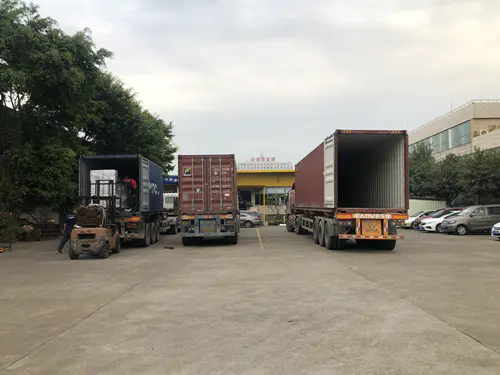
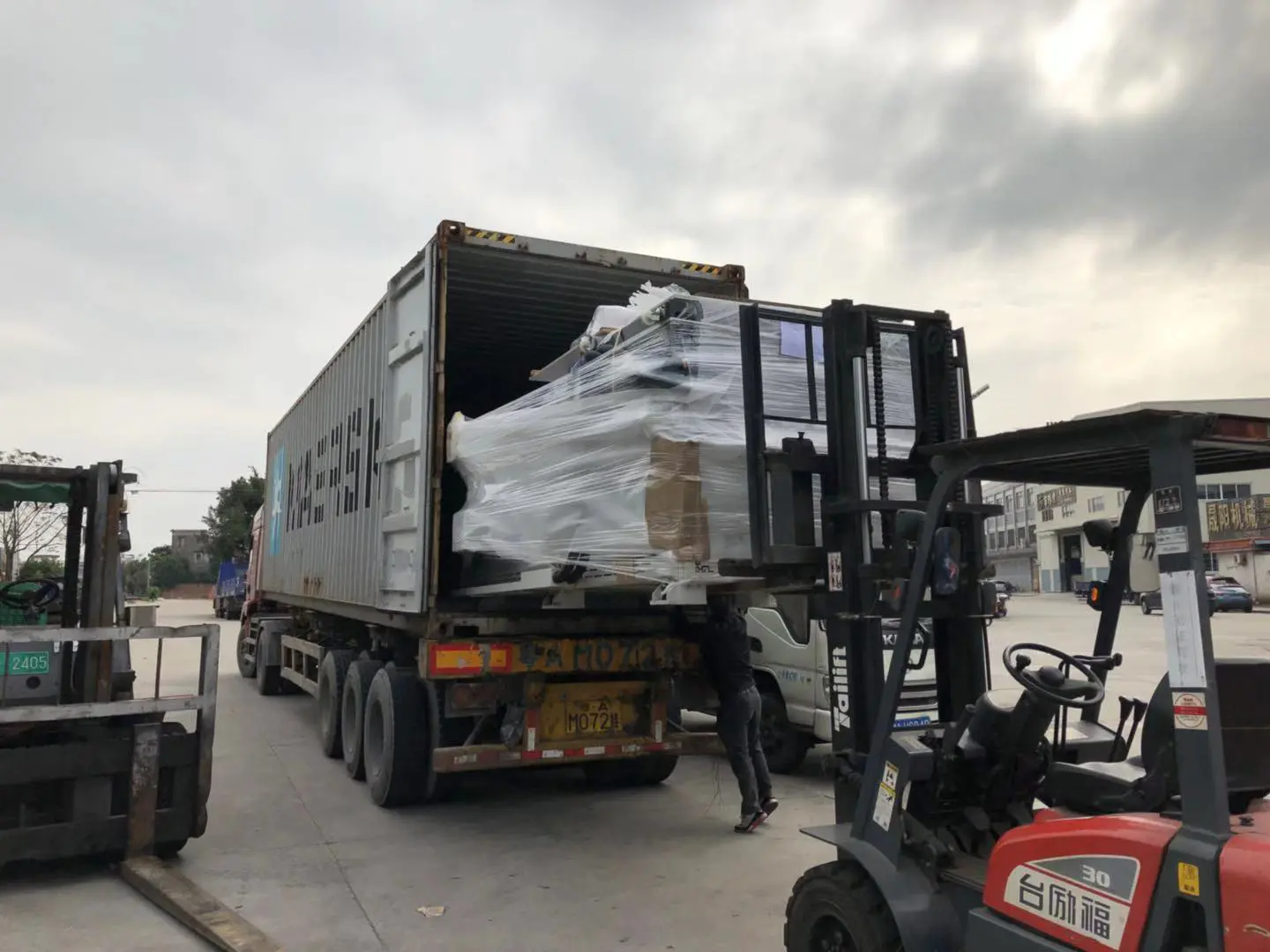
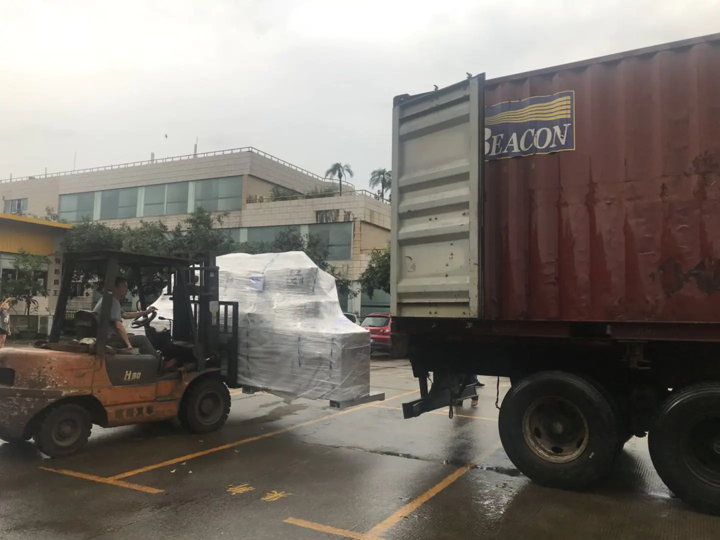
Shipment of CNC Machines
Products
how to build a usbtiny isp programmer : by utilizing cnc pcb milling machine
by:Gewinn
2020-06-06
Have you ever thought about how to build your own electronics project from scratch?
Doing electronics projects is so exciting and fun for us and for the manufacturers.
However, most manufacturers and hardware enthusiasts who have just entered the manufacturer\'s culture have built their projects with development boards, breadboards and modules.
In this way, we can build a quick prototype version of the project.
But it should be in bulk, woven with a breadboard.
While using ordinary PCB boards, similar situations are messy and unprofessional!
So how can we build our project in a more convenient way?
The best way to use independent pcb for our project!
Designing and manufacturing PCB for our project is a better and convenient way to express your professional spirit and expertise! .
We can minimize the size of our project to a compatible size and custom shape, and the clean and sturdy connection of the pcb looks is some of the advantages.
So, what\'s important is how do we build a PCB that is cost effective and time effective?
We can send our design to the PCB manufacturer to make our PCB design, but it should take time to blow your pocket.
Another method is the toner transfer method using a laser printer and photo paper.
But it also takes time to test your patient level and you also need a permanent marker to patch the non-etched parts.
I use this method a lot and I hate it.
So, what is the best way?
In my case, the best way to build a PCB using a CNC milling machine.
PCB milling machine provides you with high quality PCB, it takes less time, less resources and the cheapest way to produce PCB prototypes!
So, let\'s build a USBtiny ISP programmer with a CNC milling machine!
No further action, let\'s get started! Really!
You don\'t want to buy a PCB milling machine.
Most of us don\'t have a budget to buy such an expensive machine.
I don\'t even have one.
So how do I access the machine?
Simply put, I\'m just going to a fablab, makerspace, or hackerspace in my area!
In my case, I just went to a fablab to use this machine for a cheap price.
So, find a place like fablab or makerspace where you are.
For me, the price of using a PCB milling machine is 48 cents/hour.
Prices in your area may vary.
So, like I said, you don\'t want to be rich!
Download resources for this project!
PCB milling machine is CNC (
Computer numerical control)
Machine used to make PCB prototypes.
The PCB milling machine grinds the copper part of the copper cladding to make traces and pads of the PCB.
Three PCB milling machines-
Mechanical movement of shaft (X, Y, Z).
For precise motion, each shaft is controlled by a stepping motor.
The motion of these axes is passed by a computer program to G-code commands.
Gcode is a widely used CNC programming language that is used by most machines
Code that controls the axis of the machine. A tool head (
Generally milling position)
The pcb attached to these axes will be worn out. :-
The machine in use is the MODELA MDX20 CNC milling machine.
Modela MDX20 is a PCB milling machine.
Modela MDX20 is usually used to make pcb, but we can also make molds, etching, etc. . .
Modela can be ground on different materials such as plywood, wax, acrylic, different PCB materials such as Fr1 Fr4, etc. . .
Modela is light in weight and small in size.
We can even put it on a small desktop. The bed (Milling surface)
Attached to Y-
The shaft and the knife head are connected to X and Z.
This means that the movement of the bed is made by Y-
The shaft and movement of the knife head are controlled by X
Shaft and knife head controlled by Z-axis.
Modela has its own computer program.
But I\'m using a Linux program called FABModules.
FABmodules communicate with Modela to control the cutting and milling process.
Fab modules will never set X, Y, z-axis automatically, we need to set them manually.
In this case, a FabISP programmer if I want to make my PCB.
First of all, I need a PCB design layout and a PCB profile layout.
There are two kinds of PCB milling. stage process.
In the first Phase I need to grind out the traces and pads of the PCB and in the second phase I need to cut the PCB profile.
Use fab modules that we can convert.
Png PCB design layout for G-code. The G-
The code contains the coordination and tool path of the manufacturing PCB. The .
The Png image should be a combination of black and white colors.
The milling machine will grind out the white part using the tool head, and the black part will remain the same.
So the marks and mats should be black.
In the system programmer (ISP)
Also known as In-
Serial programmer of circuit (ICSP)
Is a controller programmer.
The ISP will read the instructions and commands from the computer USB and send them to the micro controller via the Serial Peripheral Interface (SPI).
Simply put, the ISP device allows us to communicate with the micro-controller using the SPI line.
SPI is the way of communication in the micro controller.
Each connected peripheral and interface communicates with the micro-controller via SPI.
As an electronics enthusiast, the first thing I think about when it comes to ISP is MISO, MOSI SCK.
These three pins are important pins.
Simply put, the ISP is used to burn the program to a micro-controller and also to communicate with the micro-controller!
USBTiny ISP is a simple open
USB and SPI interface.
It\'s low cost, easy to make, great to work with avrdude, AVRStudio-
Compatible and tested under Windows, Linux, and MacOS X.
Perfect for students and beginners, or as a backup programmer.
All components use SMD components in this project.
The brain of USBTinyISP is an Attiny45 micro-controller.
The micro-controller used in USBTinyISP is Attiny 45.
Attiny45 is a high-performance, low-power 8-
The bit micro-controller running on the thin architecture of Atmel (
Recently, the micro-chip acquired Atmel).
Attiny 45 is in an 8-pin package.
Attiny 45 has 6 I/O pins, 3 of which are ADC pins (10 bit ADC)
The other two are digital pins that support PWM.
It is equipped with a flash memory of one month km, 256-
System programmable memory and 256B memory.
The operating voltage is around 1. 8V to 5. 5v 300mA.
Universal serial interface is supported.
SMD version and THT version are available on the market.
Attiny 85 is a higher version of Attiny 45 and they are almost the same.
The only difference is flash memory, Attiny 45 has 4KB flash and Attiny 85 has 8KB flash.
We can choose either Attiny 45 or Attiny 85, which is not a big deal, but Attiny 45 is enough for FabTinyISP.
Check the official documents from here.
Now let\'s make the PCB using the PCB milling machine.
I have track layout and cut layout included in the zip file, you can download the zip file from below.
First, the working plate of the PCB milling machine (Milling Machine)
It\'s a metal plate.
It is solid and well built.
But in some cases it may be damaged when the depth is cut incorrectly.
So, I put a sacrifice layer on top of the milling machine (a copper-
The cladding placed on the top of the milling bed to avoid contact with the bit in the metal plate).
After placing the sacrifice layer, now I need to fix the milling bit (
Usually 1/62 milling bits are used)
On the tool head.
I already explained it.
The stage process of grinding pcb.
To mill the track and pad of the PCB, use a 1/64 milling drill bit and place it on the tool head using the Allen key.
While changing the bit, always give extra care to the point.
The tip of the drill bit is so thin that even if it is a small fall, it has more chances to break the drill bit when it slides off our hands.
To overcome this situation, I dropped a small piece of foam on the tool head to prevent accidental falls.
I use FR1 copper bag for this project. The FR-
1 heat resistant, more durable.
But copper will be oxidized soon.
The Copper Cup is a fingerprint magnet.
So before using the copper cladding, even the new copper cladding, I suggest you clean the PCB with a PCB cleaner or acetone before and after grinding the PCB.
I used a PCB cleaner to clean the PCB.
After cleaning the copper bag, place the copper bag on the top of the milling bed.
I put the copper bag on the grinding plate with the help of double sided tape. The double-
Double sided tape is very easy to disassemble and cheap.
I glued the double sided tape to the top of the sacrifice layer.
Then place the copper bag on top of the tape.
Power on the machine, and then turn on the Fab module software in the Linux system (
I use Ubuntu)
Type the following command in the Linux Terminal.
A new window will pop up. Select image(. png)
The input file format and output format are Roland MDX-20 mill(rml).
After that, click the make _ png _ rml button.
Select the bit to use at the top of the new window.
Then load your.
Png format for Clink Load. png button.
Then click Make.
Path button, generate path for mill.
Click Make now.
Rml generates instructions and commands for the machine.
A new Send it button appears at the top. rml button.
Don\'t click the button now.
We haven\'t finished yet.
Now press the View button on the Modela MDX20 control panel.
Make sure the bite is tight.
Press the View button again to go back to the default position.
Now set the X, Y position by entering the measured value (
Depending on your board position)
In the required text box.
I suggest you take note of the X & Y location somewhere.
If something goes wrong, you need to start with the first one and you should need the exact X & Y position to continue your milling process or it will go wrong.
Press the down button to remove the tool head.
Stop when the tool head is close to the copper cladding.
Then, lose the tool head screw and put it down a little until it touches the copper layer of the copper cladding.
Then tighten the screw again and put the tool head back in place by pressing the View button. Now we all set.
Close the security cover of Modela and click the send button.
The milling process will begin with Modela.
It takes at least 10 to 13 minutes to grind marks and pads.
I got a good result after finishing the milling.
After finishing the trace milling, cut out the PCB profile layout (
Simple shape of PCB).
The process is almost the same.
To cut the layout, change the 1/64 bits in the knife head to 1/32 bits.
Then load the cut layout.
Png file to fab module and select cut bit (1/32)
In the Tools menu.
Then go ahead with the same program I did before.
Take out the finished PCB from the bed.
The following is a Milled PCB!
Now I have finished the PCB.
All I need to do is weld the components on the PCB.
It\'s a fun and easy task for me.
When it comes to welding, pass-
The hole assembly is very easy to weld compared to the SMD assembly.
The size of the SMD element is small.
Welding is a bit difficult for beginners.
There are many opportunities to make mistakes, such as cold welding misplacement parts and the most common things, or building bridges between traces and pads.
But everyone has their own welding tips and tricks that are learned from their own experience.
This will make the task interesting and easy.
So, take the time to weld the parts!
I usually weld the micro controller and other ic first.
Then I weld small parts like resistors and capacitors. . . Finally through-
Hole Assembly, wire and head pin.
In order to weld my USBTinyISP, I follow the same steps.
To easily weld SMDs, first I heat the soldering iron to 350 °c.
Then add some flux to the pad.
Then heat the pads I want to weld the Assembly and then add a small amount of welding to the individual pads of the Assembly pads.
Pull out the assembly and place it on the mat using tweezers, heat the mat 2-4 second.
After that, weld the remaining pads.
If you bridge between the pin and the trace, or provide a large amount of welding to the assembly, use the welded Wick belt to remove unwanted welding.
I proceed with the same steps until the PCB is fully soldered without any problems.
If something goes wrong, first of all, I use a magnifying glass and a multimeter to carefully check all the marks and components that have broken or bridge.
If I find out, then I will rectify!
Connect the micro controller or other ISP programmer to flash the firmware.
We need a six-wire ribon line with two 2x3 bus connectors.
I used a 4/3-foot 6-channel ribbon wire to carefully connect the female heads on both sides.
I used a G clip to do better.
Look at the picture.
Now we can flash the firmware to our ISP.
We need another ISP programmer to do this.
I used another USBTinyISP, but you can do this with Arduino as an ISP.
Connect two ISPs using the ISP connector we made previously.
Then connect to USBinyISP (
The one we used to program)
To the computer.
By typing the following command in the Linux Terminal, make sure that the ISP is detected in the system.
First, we need to install the toolchain.
To do this, open the Linux Terminal and type.
Download and decompress the firmware file now.
You can download it from here
After downloading the zip file, extract to a good location that you can easily find (
Avoid unnecessary confusion).
Before burning the firmware
We need to make sure that the makefile is configured for the Attiny micro-controller.
To do this, open the Makefile in any text editor.
Then confirm MCU = attiny45.
See below.
Now we can flash the firmware to our ISP.
As I said earlier, we need another ISP programmer for this.
I used the FabTinyISP I made before.
However, you can use any ISP or Arduino as an ISP programmer.
Connect two ISPs using the ISP connector I made previously.
Then connect to FabTinyISP (
The one I used to program my ISP)
To the computer.
By typing the following command in the Linux Terminal, make sure that the Isp is detected in the system.
Now we are ready.
Open the terminal located in the folder path of the firmware and type \"make\" to create it. hex file.
This will produce one.
We need to burn to a hex file in Attiny 45.
Type the following command in the Linux Terminal to flash the firmware to the micro controller.
Start the terminal of the internal fuse.
Now we need to remove the jumper or disable the RESET pin.
Removing the jumper connection is not mandatory and we can disable the RESET pin.
It depends on you.
I chose to disable the RESET pin.
If you want to disable reset pin, type make the following command in terminal \".
You will get a message of success.
After uploading the firmware successfully, I need to check whether the USBTinyISP is working properly. For this reason, after entering the command, I need to enter the command at the terminal and will get back feedback in the terminal window.
Now you can remove both devices from your computer and program for your micro-controller from now on using the now built USBtiny.
I am using this ISP to refresh my Arduino sketch.
Custom message
Related Products